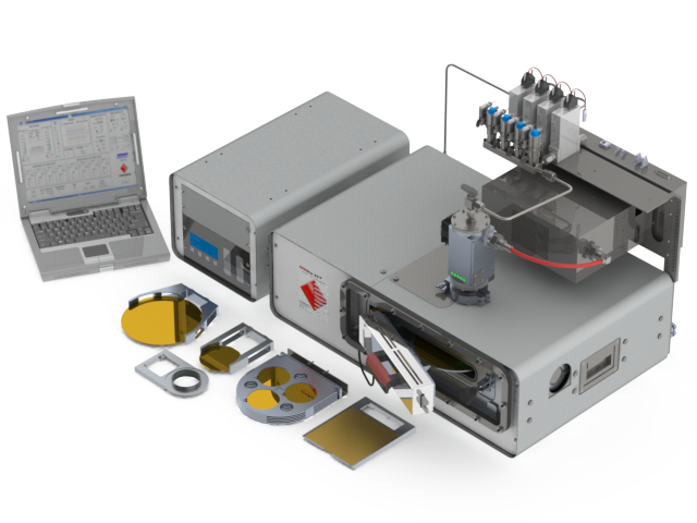


The VPG 300 DI is a Volume Pattern Generator specially designed for direct writing high-resolution microstructures in i-line resists. Derived from the mask making tool, it features all advanced VPG+ system components to be able to write with the highest precision and accuracy. The maximum write area covers a 300 mm wafer.
The target usage of the VPG 300 DI system is primarily in academic and industrial research and development, where high flexibility and features smaller than 2 µm are required. This system caters to the needs of various applications, including product prototyping, MEMS, mix and match with other tools, and writing of structures with quasi-stitching-less unlimited die sizes. The VPG 300 DI performance is comparable to a mask-based i-line stepper that is traditionally used for these applications, while providing the advantages of a maskless patterning technology.
Similar to the VPG+, the VPG 300 DI is based on the same field-proven ultra-high-speed exposure optical engine. However, it goes a step further by incorporating additional advanced system components such as a Zerodur® stage, differential interferometer, and various options for metrology, alignment, and wafer handling.
This combination of performance, technological benefits, and components makes the VPG 300 DI an ideal choice for researchers and developers seeking precise and efficient microstructure fabrication capabilities.
| Write mode | I | II |
|---|---|---|
| Writing performance | ||
| Minimum feature size [µm] | 0.5 | 0.8 |
| Minimum lines and spaces [µm] | 0.8 | 1.2 |
| Address Grid [nm] | 4 | 8 |
| Edge roughness [3σ, nm] | 30 | 40 |
| CD uniformity [3σ, nm] | 50 | 60 |
| 2nd layer alignment (global) [nm] | 100 | 130 |
| Write speed [mm2/min] | 340* | 1020* |
| *Fast mode: 680 and 2056 mm2/min with similar performance, but without specification | ||
| Exposure time for 100 x 100 mm2 area [min] | 39 | 17 |
| System features | ||
|---|---|---|
| Light source | High-power DPSS laser with 355 nm | |
| Maximum substrate size and write area | 300 x 300 mm2 | |
| Substrate thickness | 0 to 12 mm (other thicknesses on request) | |
| Maximum exposure area | 300 x 300 mm2 | |
| Autofocus | Realtime autofocus system (optical and pneumatic) | |
| Autofocus compensation range | Up to 80 µm | |
| Flowbox | (Closed-loop) temperature controlled environmental chamber | |
| Alignment and metrology | Camera system and software package for metrology and alignment | |
| Other features and options | Full automatic handling and prealigning of 100, 150, 200, and 300 mm wafers. Optical edge detection, topside alignment and optional IR and backside alignment. Zerodur® stage and high-resolution differential interferometer | |
| System dimensions | ||
| System / Electronic rack | ||
| Width [mm] | 2605 / 800 | |
| Depth [mm] | 1652 / 650 | |
| Height [mm] | 2102 / 1800 | |
| Weight [kg] | 3550 / 180 | |
| Installation requirements | ||
| Electrical | 400 VAC ± 5 %, 50/60 Hz, 16 A, 3 phases | |
| Compressed air | 6 - 10 bar |
Please note
Specifications depend on individual process conditions and may vary according to equipment configuration. Write speed depends on pixel size and write mode. Design and specifications are subject to change without prior notice.
Subscribe today to hear first about our new and exciting technology


