MLA300 Maskless Aligner for Volume Production

MLA300 Maskless Aligner for Volume Production - Nano Vacuum Australia & New Zealand

MLA300 Maskless Aligner for Volume Production

Your inquiry was submitted successfully. You can expect to hear from us shortly.

OPTIMIZED FOR INDUSTRIAL MANUFACTURING, ENSURING HIGH THROUGHPUT AND SEAMLESS PRODUCTION LINE INTEGRATION

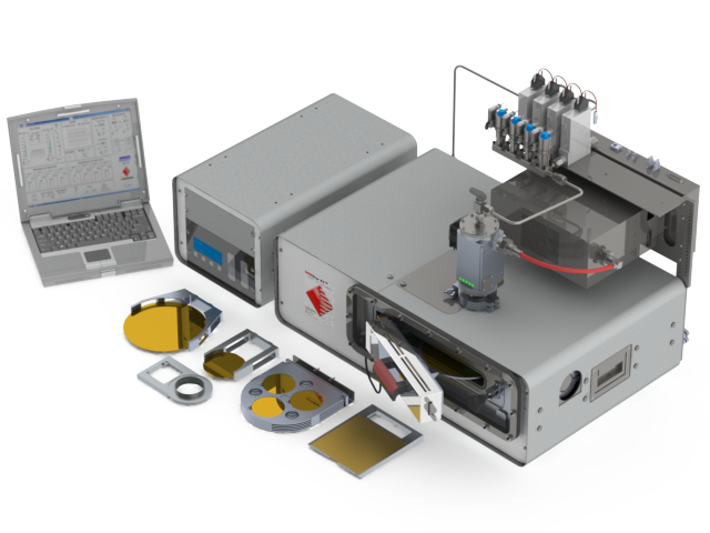
The Maskless Aligner MLA300 provides high throughput, simplified workflow and integration with manufacturing execution systems (MES). This tool is used for the production of sensors and sensor ICs, MEMS and microfluidic devices. Other applications include discrete electronic components, analog and digital ICs, ASICs, power electronics, OLED displays and advanced packaging.

The MLA300 achieves the highest optical quality and precision. The standard exposure module achieves min. feature size of 1.5 µm. Writing modes for higher throughput at 4 µm resolution and higher resolution at 1 µm are coming soon. MLA300 features full automation with customizable loading options, software designed for production environments and a patented substrate tracking technology.

The MLA300 reduces production costs and effort by overcoming the requirement for mask procurement, verification and management. Operating costs benefit from a long-lifetime exposure laser (est. 10 years at 24/7 production) and fewer consumables. Modularity enables fast maintenance, replacement or repair. Real-time autofocus compensates substrate warp or corrugations for flawless patterning. Maskless lithography allows per-die pattern corrections and serialization for full tracing of product characteristics, such as sensor calibration.

Direct-write Lithography

No mask-related costs, effort, or security risks

Flexibility

Direct writing in industrial production allows per-die pattern corrections, e.g. to react to distortions or process variations and serialization

Time-saving

Shorter time from prototyping to production. Digital design management replaces conventional mask library

Exposure Quality

Optical compensation of scaling, rotation; patented substrate tracking technology

Dynamic Autofocus

Superior critical dimensions (CD) uniformity on warped or corrugated substrates

Exposure Speed

300 x 300 mm in 19 minutes

Full Facility Integration

Customizable automatic loader, substrate chuck including warped substrates, custom workflow “wizards” and interface with manufacturing execution systems (MES)

User-friendly

SEMI-compliant user interface; customized workflow “wizards” for system operators

Low Cost of Ownership

Laser lifetime 10 years at 24/7 operation. Power consumption Eur 11,667 per year at 0.2 Eur/ kWh. Filters and replacement parts 5,400 Euro/year

Automated Loading Module

SEMI-standard BOLTS plane can be configured for open cassettes or Load Ports for FOUP. The number and configuration of ports can be selected and customised for round or rectangular substrates

Exposure Modules

High- throughput write mode with 4 μm resolution available from Q2 2021; high-resolution write mode with 1 μm resolution available from Q3 2021

Manufacturing Execution System (MES)

Integration Customizable workflow “wizards” to start exposure jobs, and integration to a central MES via SECS/GEM or OPC-UA protocols

Backside Alignment

Visual or through-wafer IR backside alignment available with 1 um positioning accuracy

Exposure Wavelengths

High-power diode lasers at 375 nm or 405 nm are available

Service Contracts

Service contract grades for faster on-site support and participation in the spare parts pool
Writing performance
Minimum lines and spaces [µm] 2
Minimum feature size [µm] 1.5
CD uniformity [3σ, nm] 200
Edge roughness [3σ, nm] 80
Stitching [3σ, nm 120
2nd layer alignment [3σ, nmσ] 500
Backside alignment [3σ, nm] 1000
Exposure time per module ( 100 x 100 mm² at 50 mJ/cm² and 405 nm laser wavelength) 2.6 min
Maximum write speed with one module at 405 nm laser wavelength 5000 mm²/min

System features
Light source Laser wavelength: 375 nm and 405 nm High power diode laser with long life-time
Maximum substrate size 300 x 300 mm²
Maximum exposure area 300 x 300 mm²
Substrate thickness 0.1 - 10 mm
Modular environmental chamber Temperature stability ± 0.1°C
Real-time autofocus Optical and/or pneumatic autofocus
Autofocus dynamic range Up to 150 µm
Alignment Advanced alignment; backside alignment optional
Automation Automatic wafer handling and pre-alignment
System dimensions (excluding loader)
Height × width × depth 1980 mm x 1200 mm x 2310 mm
Weight 2600 kg
Installation requirements
Electrical 400 VAC, 50/60 Hz, 16 A

Please note
Specifications depend on individual process conditions and may vary according to equipment configuration. Write speed depends on pixel size and write mode. Design and specifications are subject to change without prior notice.

DOWNLOAD FACTSHEET

    This site is protected by reCAPTCHA and the Google Privacy Policy and Terms of Service apply.

    You may also like


    Recently viewed