Heidelberg Instruments MLA150 Direct Write Maskless Aligner - Nano Vacuum Australia & New Zealand

MLA150 Direct Write Maskless Aligner

Heidelberg Instruments SKU: MLA150
  • In stock, ready to ship
  • Backordered, shipping soon
  • Estimated Leadtime = days
Your inquiry was submitted successfully. You can expect to hear from us shortly.

THE FASTEST MASKLESS TOOL FOR R&D, RAPID PROTOTYPING AND SMALL PRODUCTION VOLUMES, DESIGNED FOR BINARY LITHOGRAPHY

The Maskless Aligner MLA150 – now how high-resolution mode!

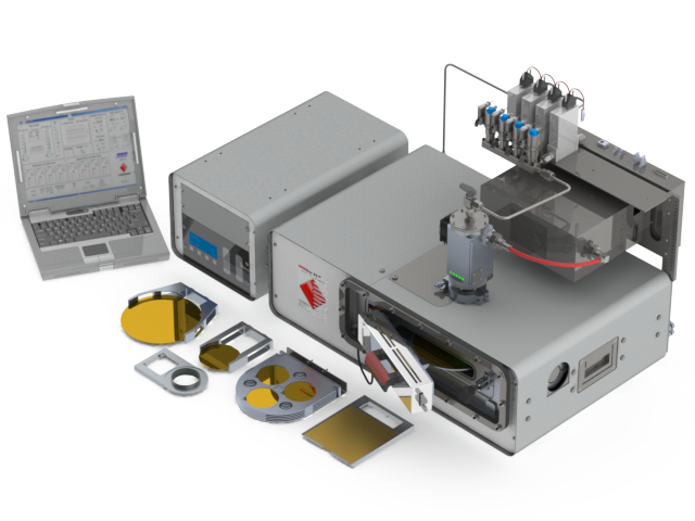
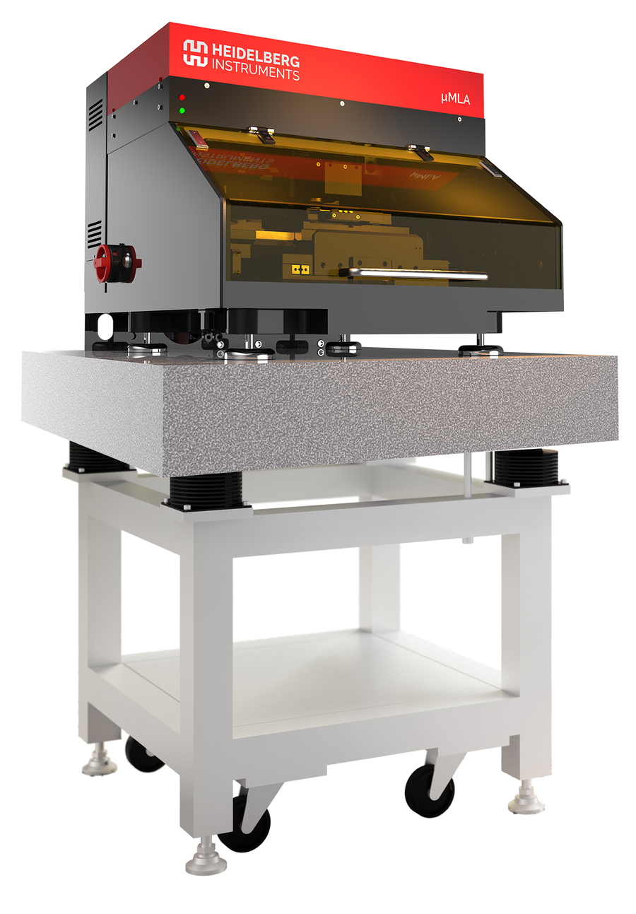
Maskless Aligner MLA150 is a state-of-the-art maskless lithography tool. Areas of application include nanofabrication of quantum devices (2D materials, semiconductor materials, nanowires, etc) MEMS, micro-optic elements, sensors, actuators, MOEMS and other devices for materials and life sciences. Depending on the application, MLA150 patterns high-resolution, high aspect ratio, and even simple grayscale structures

Our Maskless Aligner series, first introduced in 2015, is now firmly established as an alternative to the traditional Mask Aligner, fully eliminating the need for masks. The maskless approach leads to significantly reduced cycle times. Any design modifications can be quickly implemented by simply changing the CAD layout. The system also features fast automated front- and backside alignment procedures and outstanding speed: Exposing an area of 100 x 100 mm² with structures as small as 1 micron takes less than 10 minutes.

Customer Testimonial

I had been using the MLA150 for almost 5 years. It was definitely one of the most popular tools in our cleanroom. Once people got to know the MLA – no one wanted to go back to a mask aligner or stepper. The best thing about the MLA150 is its flexibility – the tool can work with samples of different shapes and sizes, and new designs can be added very easyly. The software is very intuitive and easy to learn. Moreover, the service team had always provided us with exceptional support, all issues were quickly resolved. I highly recommend Heidelberg Instruments and their products.
Anna Mukhortova, Pritzker Nanofabrication Facility - UNIVERSITY OF CHICAGO

Perfect for Multiuser Facilities

Training <1 h to fully qualify as a user

Fast and Accurate Alignment

250 nm front alignment, backside alignment, alignment error compensation

Flexible

2 lasers can be installed simultaneously on the same system to expose the whole range of photoresists

Low Operation Costs and Easy Maintenance

10-20 years of laser lifetime

Direct-write Lithography

No mask-related costs, effort, or security risks

Grayscale Mode

For simple 2.5D structures

Exposure Quality

Edge roughness 60 nm; CD uniformity 100 nm; 40 nm address grid; autofocus compensation for warped/corrugated substrates

User-friendly

Specifically designed software and workflow make the tool operation fast and easy

Exposure Speed

150 mm wafer in <16 min with 405 nm laser

Exposure Wavelength

Diode laser sources at 375 and/or 405 nm can be mounted together and used interchangeably to expose different photoresists

Exchangeable Chucks

Custom vacuum layouts

Draw Mode

Import and overlay of .bmp files on top of the real-time microscope image — as in a virtual mask aligner; simple lines and shapes can be drawn into the real-time camera image for immediate exposure

Autofocus

Air-gauge or optical autofocus for perfect exposure of small samples (less than 10 mm)

Variable Substrate Sizes

3-6”, up to 8” upon request

Advanced Field Alignment

Automatic field-by-field alignment on individual dies on the wafer for superior alignment accuracy


Writing performance Write Mode I Write Mode II
Minimum structure size [μm] 0.6 1
Linewidth variation [3σ, nm] 100 120
Global 2nd layer alignment [3σ, nm] 500 500
Local 2nd layer alignment [3σ, nm] 250 250
Backside alignment [3σ, nm] 1000 1000
Exposure time 405 nm laser for 4″ wafer [min] 35 9
Exposure time 375 nm laser for 4″ wafer [min] 35 20
Max. write speed 405 nm laser [mm²/min] 285 1100
Max. write speed 375 nm laser [mm²/min] 285 500

System features
Light source Diode lasers: 8 W at 405 nm, 2.8 W at 375 nm, or both
Substrate sizes Variable: 3 x 3 mm² to 6″ x 6″ | Optional: 8″ x 8″ Customizable on request
Substrate thickness 0 - 12 mm
Maximum exposure area 150 x 150 mm² | Optional: 200 x 200 mm²
Temperature controlled flow box Temperature stability ± 0.1°
Real-time autofocus Air-gauge or optical
Autofocus compensation range 180 μm
Grayscale 128 gray levels
Software features Exposure wizard, resist database, automatic labeling and serialization, Draw Mode for CADless exposures, substrate tracking / history
System dimensions (lithography unit)
graphy unit) Height × width × depth 1950 mm × 1300 mm × 1300 mm
Weight 1100 kg
Installation requirements
Electrical 230 VAC ± 5%, 50/60 Hz, 16 A
Compressed air 6 - 10 bar, stability ± 0.5 bar


Economical considerations
Saves on the cost of photomasks
Low running costs for maintenance, energy consumption, spare parts
Solid state laser light sources with lifetime of several years
* Only one write mode can be installed on the system


    This site is protected by hCaptcha and the hCaptcha Privacy Policy and Terms of Service apply.

    Recently viewed