ULTRA The Semiconductor Laser Mask Writer

ULTRA The Semiconductor Laser Mask Writer - Nano Vacuum Australia and New Zealand

ULTRA The Semiconductor Laser Mask Writer

Your inquiry was submitted successfully. You can expect to hear from us shortly.

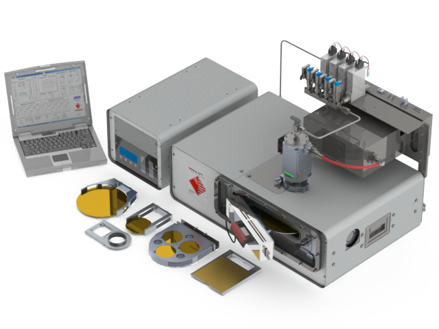
DESIGNED TO PRODUCE NON-CRITICAL SEMICONDUCTOR PHOTOMASKS FOR DESIGN NODES DOWN TO 130 NM, AND NON-MANHATTAN DESIGNS

The ULTRA specifically addresses the production of mature semiconductor photomasks. It is a qualified tool at a major semiconductor photomask production group. The ULTRA is used to fabricate semiconductor components for the electronics and automotive industries. These include power management, microcontrollers, LED lighting, the internet-of-things (IoT) and MEMS.

The ULTRA is an economical mask writer solution with all the features and functionality required for high throughput, precision and structure uniformity, and extremely accurate alignment. The standard configuration includes all modules (FX Fast mode, SMIF Pod, etc). The ULTRA can produce structure sizes down to 500 nm at write speeds up 580 mm2 per minute, while featuring excellent critical dimension uniformity, image quality, overlay and registration. ULTRA 1 produces masks down to 180 nm nodes. ULTRA 2 will be launched in late 2021 and will target significant improvement in alignment accuracy and exposure quality – aiming at 130 nm design node. ULTRA is a compact system and fits easily into the existing mask shop infrastructure.

Two Models

ULTRA 1 for 180 nm design node; ULTRA 2 for 130 nm design node

High Exposure Quality

Line edge roughness 20 nm; CD uniformity 30 nm; positioning accuracy 40 nm; real-time optical autofocus; custom high numerical aperture (NA) write-lens optimized for laser exposure

High Precision

XY stage fully designed and manufactured by Heidelberg Instruments; full air bearing stage; zero thermal expansion zerodur™ chuck; differential interferometer for position measurement

Precise Second Layer Alignment

Sophisticated correction matrix based on a 2D measurement of the first layer. Compensation of arbitrary local position distortions; 100 nm accuracy

High Throughput

High-speed SLM with high data rate for fast exposure. 150 mm wafer in < 45 minutes

Writing Stability

Closed-loop environmental chamber complies with stringent requirements for semiconductor photomask production; integrated metrology system with flowbox and software corrections compensates for any variations in environmental parameters

Long life-time

Economical high-power DPSS 355 nm laser; 20,000 hours of guaranteed lifetime

Overall Cost of Ownership

Laser power consumption ca. 25.270 EUR/year at 0.2 EUR/kWh, 90% tool operation; other consumables 38.500 EUR/year

Footprint

1.65 m x 2.54 m


Writing performance QX mode FX mode
Address grid [nm] 5 10
Line edge roughness [3σ, nm] 20 40
Position accuracy [3σ, nm] 40 100
Overlay [3σ, nm] 30 60
Stitching [3σ, nm] 20 60
2nd layer alignment [3σ, nm] 100 100
CD uniformity [3σ, nm] 30 60
Minimum feature size [nm] 500 700
Write speed [mm² / min] 325 580
Write time for 6″ x 6″ [min] 75 45

Operation
Protocols, standards SECS / GEM protocols
User interface (software) SEMI-compliant GUI
Maximum write area 228 x 228 mm²
Substrate size 4″, 5″, 6″, 7″, and 9″ masks
System features
Optics 0.9 NA objective lens; Low-distortion UV optics; Automatic calibration routines
Laser 355 nm high-power solid state laser; Highly economical compared to gas laser
Focus system Real-time optical autofocus
Alignment Camera system; Distortion compensation; Field-by-field alignment
Data path Real-time compression; Scalable hardware concept; Input formats: All standard formats, e.g. GDSII and Jobdeck
Spatial Light Modulator Frequency 350 kHz; Data rate 2.4 GB/s
Loader Automatic mask loader with two independent carrier stations
System dimensions System / Electronic rack
Width [mm] 2730 / 800
Depth [mm] 1650 / 650
Height [mm] 2100 / 1800
Weight [kg] 3400 / 180
Installation requirements
Electrical 400 VAC ± 5%, 50/60 Hz, 32 A
Compressed air 7 - 10 bar (without oil or other residue)

     Please note
    Specifications depend on individual process conditions and may vary according to equipment configuration. Write speed depends on pixel size and write mode. Design and specifications are subject to change without prior notice

    This site is protected by reCAPTCHA and the Google Privacy Policy and Terms of Service apply.

    You may also like


    Recently viewed