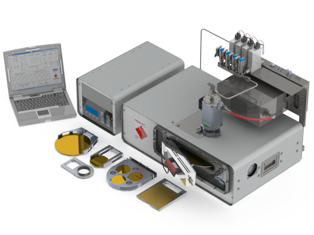


The NanoFrazor is a groundbreaking commercial system for Thermal Scanning Probe Lithography (t-SPL), enabling advanced research in various application areas such as quantum devices, 1D/2D materials, quantum dots, Dolan bridges, Josephson junctions, and nanoscale arrays. It excels in complex applications such as grayscale photonics, nanofluidic structures, biomimetic substrates for cell growth, and any local material modification through heat, including chemical reactions and physical phase changes.
At its core, the NanoFrazor features an ultra-sharp, heatable probe tip that writes and inspects complex nanostructures simultaneously. The Direct Laser Sublimation (DLS) module allows nano- and micro-structures to be written into the same resist layer efficiently in a single fabrication step.
In-situ imaging enables two unique features: markerless overlay and comparison of the written and target patterns during writing, in such a way that the parameters can be immediately adjusted. This approach, called Closed-Loop Lithography (CLL), results in sub-2 nm vertical precision for 2.5D (grayscale) shapes of any complexity. Fast and precise control of a heated nanoscale tip enables innovation not otherwise feasible with other techniques.
Developed from over 20 years of R&D at IBM Research Zürich and now at Heidelberg Instruments Nano, the NanoFrazor continuously advances in hardware and software. Our experts refine pattern transfer processes like etching and lift-off for various applications, compiling expertise into a comprehensive library of best practices and protocols to support our customers.
Built on a modular platform, the NanoFrazor can be tailored to fit specific applications and laboratory environments. Patterning modes, housing options, and software modules can be combined for optimal capabilities, footprint, and flexibility. Upgrades and additional modules can be added as research evolves, ensuring the NanoFrazor adapts to advancing needs.
The NanoFrazor revolutionizes nanofabrication, making sophisticated t-SPL accessible for groundbreaking research and technological advancements.
| Thermal Probe Writing | Direct Laser Sublimation | ||
|---|---|---|---|
| Single Tip | Decapede | ||
| Patterning performance | |||
| Minimum structure size [nm] | 15 | 15 | 600 |
| Minimum Lines and Spaces [half pitch, nm] | 25 | 25 | 1000 |
| Grayscale / 3D-resolution (step size in PPA) [nm] | 2 | 2 | - |
| Maximum writing field size [X μm x Y μm] | 60 x 60 | 60 x 60 | 60 x 60 |
| Field stitching accuracy (markerless, using in-situ imaging) [nm] | 25 | 25 | 600 |
| Overlay accuracy (markerless, using in-situ imaging) [nm] | 25 | 25 | 600 |
| Write speed (typical scan speed) [mm/s] | 1 | 1 | 5 |
| Write speed (50 nm pixel) [μm²/min] | 1000 | 10 000 | 100 000 |
| Topography imaging performance | |||
| Lateral imaging resolution (feature size) [nm] | 10 | ||
| Vertical resolution (topography sensitivity) [nm] | <0.5 | ||
| Imaging speed (@ 50 nm resolution) [μm²/min] | 1000 | 10 000 | - |
| Base system features | |
|---|---|
| Substrate sizes | 1 x 1 mm² to 100 x 100 mm² (150 x 150 mm² possible with limitations) Thickness: up to 10 mm |
| Optical microscope | 0.6 μm digital resolution, 2 μm diffraction limit, 1.0 mm x 1.0 mm field of view, autofocus |
| Magnetic cantilever holder | Fast (<1 min) and accurate tip exchange |
| Vibration isolation | Active vibration isolation stage |
| Optional system features / modularity | |
| Direct laser sublimation | Laser source and optics: 405 nm wavelength CW fiber laser, 300 mW, 1.2 μm minimum focal spot size Laser autofocus: Using the distance sensor of the NanoFrazor cantilever |
| Decapede | Parallel writing with 10 tips |
| Standalone housing | Three-layer acoustic isolation, superior vibration isolation (> 98% @ 10 Hz) | PC-controlled temperature and humidity monitoring, gas-flow regulation | (Dimension 185 cm x 78 cm x 128 cm / weight 650 kg) |
| Full glovebox integration | Integration in glovebox available for nanolithography in a controlled environment |
| NanoFrazor cantilever features (both Single Tip and Decapede) | |
| Integrated components | Tip heater, topography sensor, electrostatic actuation |
| Tip geometry | Conical tip with <10 nm radius and 750 nm length |
| Tip heater temperature range | 25 °C – 1100 °C (<1 K setpoint resolution) |
| Base system dimensions & installation requirements | |
| Height × width × depth | Table-top unit: 44 cm x 40 cm x 45 cm Controller: 84 cm x 60 cm x 56 cm |
| Weight | Table-top unit: 50 kg Controller: 80 kg |
| Power input | 1 x 110 or 220 V AC, 10 A |
| Software features | |
| GDS and bitmap import, 256 grayscale levels, topography image analysis and drawing for overlay, mix & match between tip and laser writing, fully automated calibration routines, Python scripting |
Subscribe today to hear first about our new and exciting technology
