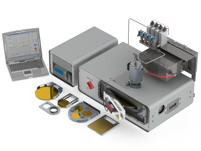
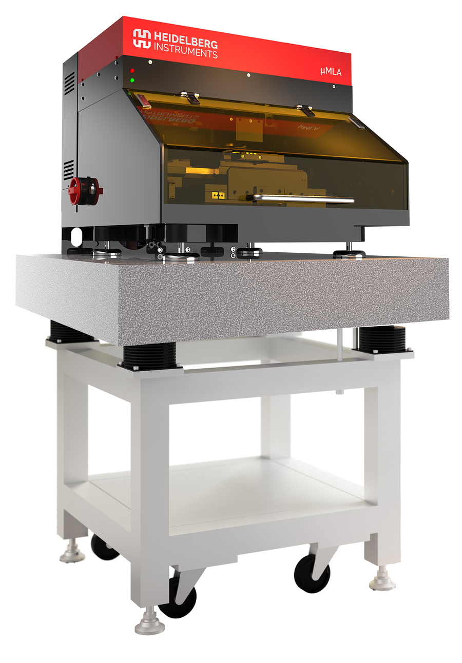
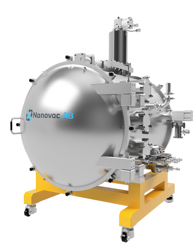
Ion beam etch offers maximum flexibility coupled with excellent uniformity and is suitable for a wide range of applications. Our systems have flexible hardware options including open load, single substrate load lock and cassette to cassette. System specifications are closely tuned to applications, enabling faster and repeatable process results.
-
Multiple mode functionality
- Capable of clustering with other plasma etch and deposition tools
- Single wafer loadlock or cluster wafer handling
- Dual-beam Configuration
- Very low surface film roughness
- Unmatched batch uniformity and process reproducibility
- Accurate end point detection – SIMS, optical emission
Features & Benefits
- High quality thin film - Ultra low contamination
- High throughput with reduced footprint - Low cost of operation
- Patented high speed substrate holder (up to 1000 RPM) equipped with a white light optical monitor design - Very accurate in-situ optical film control
- Flexible configuration - Advanced research applications
- Flexible wafer handling capability - Open load, single wafer load lock or cassette-to-cassette robotic handler
Options
Ion Beam Etching Modes
- Ion beam etching (IBE)
- Reactive ion beam etching (RIBE)
- Chemically assisted ion beam etching (CAIBE)
Ionfab300 Standard Chamber
A compact ion beam etch and deposition system designed for flexible research and pilot production, equipped with up to two (15cm) ion sources for etch or deposition. This makes it ideal for deposition on up to 200mm wafer size and etch process optimised for up to 100mm wafer size.
Ionfab300 Large Chamber
Having essentially the same footprint but with a larger process chamber, it is designed to process wafers up to 200mm for both etch and deposition. Equipped with a 30cm etch ion source, the system provides excellent etch uniformity and superior process stability, making it a great choice for pilot and full scale production.
Applications
- Magnetoresistive random access memory (MRAM)
- Dielectric films
- III-V photonics etching
- Spintronics
- Metal contact and track
- Superconductors
- Laser facet coating
- High reflection (HR)
- Anti-reflection (AR)
- Ring laser gyroscope mirrors
- X-ray optics
- Infrared (IR) sensors
- II-VI -based
- Telecom filters


