μMLA The Table-Top Maskless Aligner

μMLA The Table-Top Maskless Aligner-Nano Vacuum Australia and New Zealand

μMLA The Table-Top Maskless Aligner

Your inquiry was submitted successfully. You can expect to hear from us shortly.

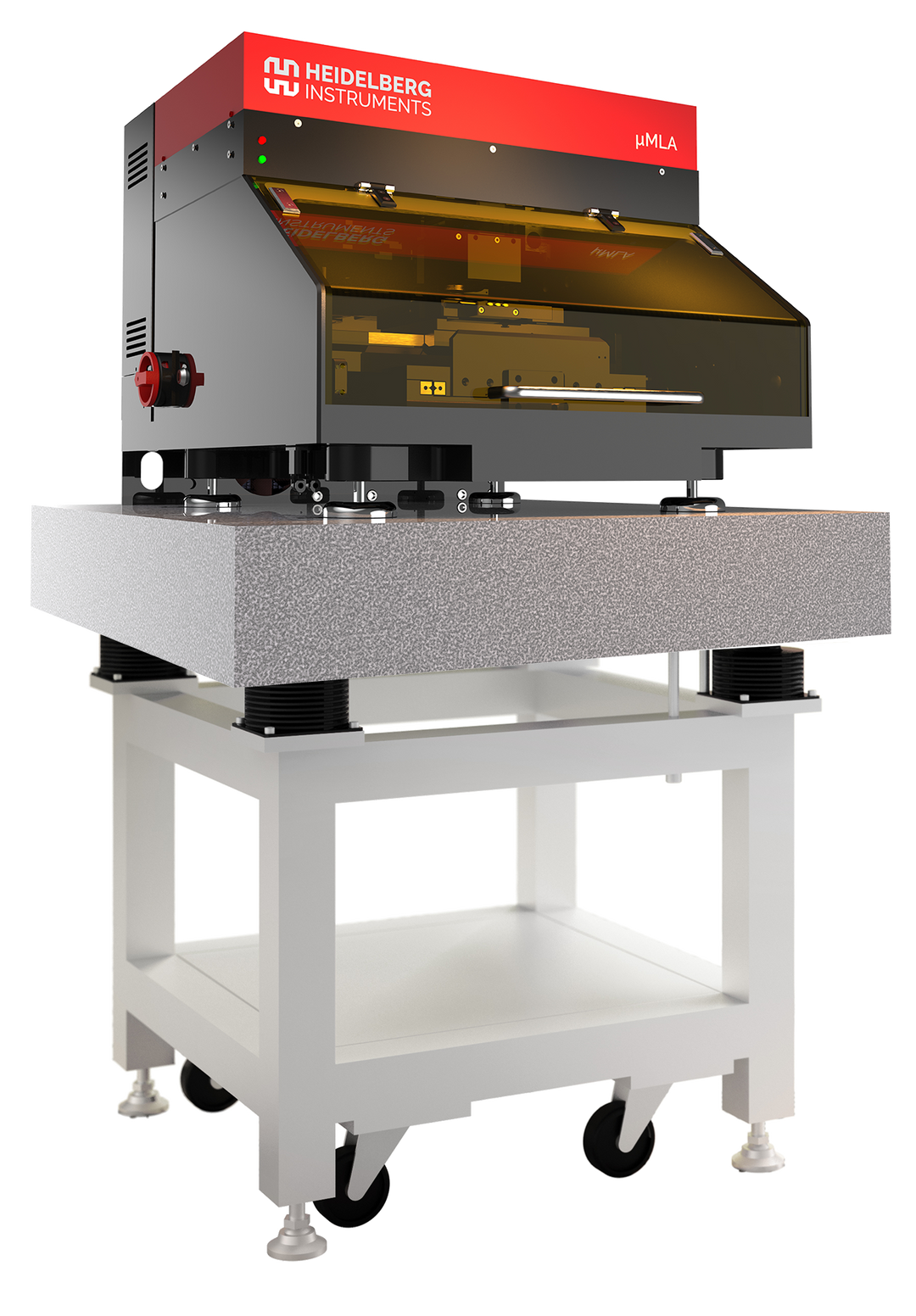
CONFIGURABLE AND COMPACT TABLETOP MASKLESS ALIGNER WITH RASTER SCAN AND VECTOR EXPOSURE MODULES

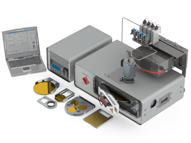
The tabletop µMLA system is state-of-the-art in maskless technology built on the renowned µPG platform – the most sold tabletop maskless system worldwide. It is a perfect entry-level research and development (R&D) tool for virtually any application requiring microstructures. Typical examples are microfluidics (cell sorting devices, lab-on-a-chip), small-scale mask-writing, micro-optics and microlens arrays, sensors, MEMS, contacting 2D materials and fan-out electrodes, etc.

The µMLA is a flexible and customizable tool, and offers two exposure modes. The standard µMLA uses the Raster Scan Exposure Mode for exposures, which is fast and provides excellent image quality and fidelity, while the write time is independent of structure size of pattern density. The optional Vector Scan Mode is designed for patterning continuous smooth curves such as waveguides in a faster and more accurate way. Three optical setups offer a choice of variable resolution and throughput. Each allows easy switching between different resolution and speed configurations to optimize exposure for a given application. The Draw Mode enables straightforward ad-hoc modifications to existing structures and electrical contacts to nanowires or 2D materials. The grayscale exposure mode allows the creation of complex 2.5 structures such as micro-optical devices. With its small footprint, the µMLA fits on a regular table.

TECHNICAL DATA

Write Mode I * Write Mode II * Write Mode III *
Writing performance (Raster Scan Exposure Module)
Minimum structure size [μm] 0.6 1 3
Minimum lines and spaces [μm] 0.8 1.5 3
Address grid [nm] 20 50 100
CD uniformity [3σ, nm] 200 300 400
2nd layer alignment over 5 x 5 mm² [nm] 500 500 1000
2nd layer alignment over 50 x 50 mm² [nm] 1000 1000 2000
Write speed with 390 nm LED / 365 nm LED with 390 nm LED / 365 nm LED with 390 nm LED
Write speed 10 mm²/min at 0.6 µm 40 mm²/min at 1 µm 130 mm²/min at 3 µm
Optional write speeds at different minimum structure sizes with “Variable Resolution for Raster Scan Exposure Module” 18 mm²/min at 1 µm 60 mm²/min at 2 µm 160 mm²/min at 4 µm
25 mm²/min at 2 µm 90 mm²/min at 4 µm 300 mm²/min at 6 µm
Writing performance (Vector Mode Exposure Module)
Minimum feature size [µm] 0.6 1 3
Address grid [nm] 20 20 20
2nd layer alignment over 5 x 5 mm² [nm] 500 500 1000
2nd layer alignment over 50 x 50 mm² [nm] 1000 1000 2000
Maximum linear write speed in Vector Mode 200 mm/s 200 mm/s 200 mm/s
Available spot sizes in Vector Mode [µm] 0.6 / 1 / 2 / 5 / 10 1 / 2 / 5 / 10 / 25 3 / 5 / 10 / 25 /50
System specifications
Maximum substrate size 6″ x 6″
Minimum substrate size 5 x 5 mm2
Substrate thickness 0.1 to 12 mm
Maximum write area 150 x 150 mm2

Raster scan exposure module Vector exposure module
Light source LED; 390 nm or 365 nm Laser; 405 nm and/or 375 nm
System dimensions (lithography unit)
µMLA Width x Depth Height x Weight
Main system housing 640 mm (25") x 840 mm (33") 530 mm (21") x 130 kg (285 lbs)
Installation requirements
Electrical 230 VAC / 6A or 110 VAC / 12A (±5%, 50/60 Hz)
Compressed air 6 - 10 bar
Cleanroom ISO 6 recommended
Temperature stability ±1 °C
* Only one write mode can be installed on the system

Please note
Specifications depend on individual process conditions and may vary according to equipment configuration. Write speed depends on pixel size and write mode. Design and specifications are subject to change without prior notice.

DOWNLOAD FACTSHEET


This site is protected by reCAPTCHA and the Google Privacy Policy and Terms of Service apply.

You may also like


Recently viewed