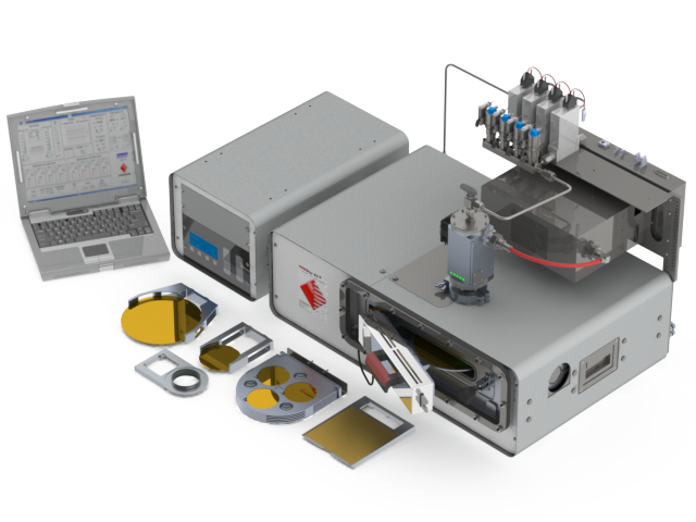
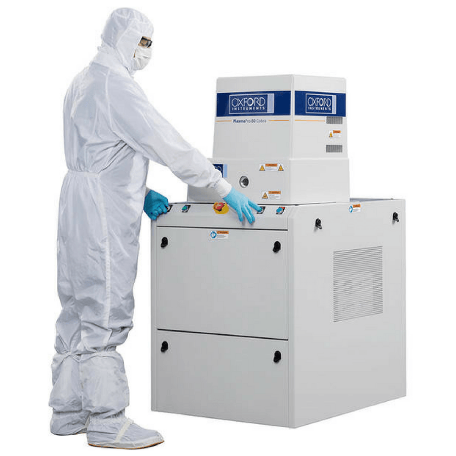
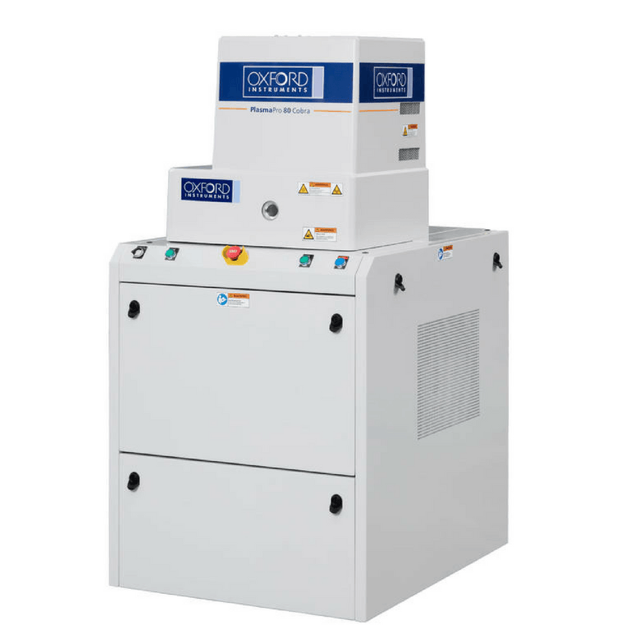
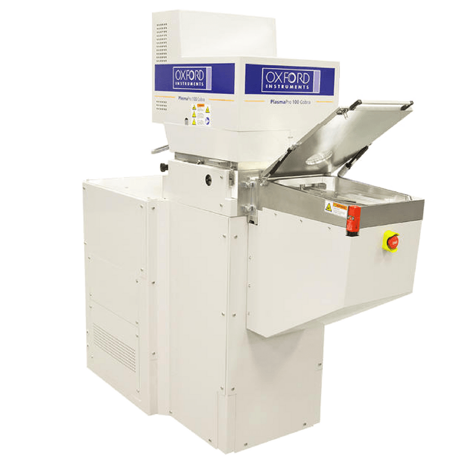
The PlasmaPro 80 is a compact, small footprint system offering versatile etch and deposition solutions with convenient open loading. It is easy to site and easy to use, with no compromise on process quality. The open load design allows fast wafer loading and unloading, ideal for research, prototyping and low-volume production. It enables high performance processes using optimised electrode cooling and excellent substrate temperature control.
- Open load design allows fast wafer loading and unloading
- Excellent etch control and rate determination
- Excellent wafer temperature uniformity
- Up to 200mm wafers
- Low cost of ownership
- Built to Semi S2/S8 standards
Features & Benefits
- Small footprint - Easy to site
- Optimised electrode cooling - Substrate temperature control
- High-conductance radial (axially symmetric) pumping configuration - Guaranteed enhanced process uniformity and rates are
- Addition of < 500ms data logging - Traceability and history of chamber and process conditions
- Close-coupled turbo pump - High pumping speed and excellent base pressure
- Clear ease of access to key components - Improved serviceability and maintenance
- X20 control system - Greatly increases data retrieval and delivers faster, more repeatable matching
- Fault and tool diagnostics via front end software - Rapid fault diagnosis
- Laser end-point detection using interferometry - Measure etch depth in transparent materials on reflective surfaces (for example, oxides on Si), or reflectometry for non-transparent materials (such as metals) to determine layer boundaries
- Optical emission spectrometry (OES) for large sample or batch process end-pointing - Detecting changes in etch by-products or depletion of reactive gas species, and for chamber clean end-pointing
Applications
- III-V etch processes
- Silicon Bosch and cryo-etch processes
- Diamond Like Carbon
- (DLC) deposition
- SiO2 and quartz etch
- Failure analysis dry etch de-processing using the specially-configured PlasmaPro FA tools ranging from packaged chip and die etch through to full 200mm wafer etch
- High quality PECVD of silicon nitride and silicon dioxide for photonics, dielectric layers, passivation and many other uses
- Hard mask deposition and etch for high brightness LED production
You may also like
More from Oxford Instruments Plasma
More from Fabrication
Recently viewed


