Why Atomic Layer Deposition & 2D Materials Are A Great Match-OXFORD Instruments
What are 2D materials and how to grow?
2D materials with thicknesses of a single atom and superlative electronic and optoelectronic properties are great candidates for next-generation devices in electronics, optoelectronics and energy applications.
In addition to graphene as the most well-known 2D material, nitrides (hBN), 2D oxides and transition metal dichalcogenides (TMDs) like MoS2, WSe2 gathered a lot of attentions.
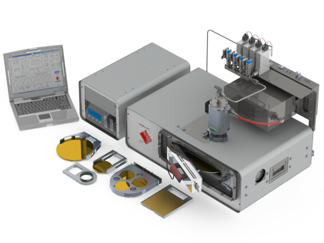
Chemical vapor-based techniques such as our high temperature (up to 1200°C) CVD, PlasmaPro 100 Nano (Nanofab), as well as lower temperature techniques (up to 600 °C) ALD, FlexAL2D, can be applied to grow high-quality 2D materials.
Why using ALD for 2D materials?
High temperature of CVD process (over 800 °C) and raise of the atom diffusion atoms is often fatal in semiconductors process. Plasma is known to yield high quality materials at lower temperatures, and this is exemplified by the deposition of MoS2 at CMOS where crystalline material was obtained at 300 °C by plasma ALD while providing a precise digital thickness and uniform growth over a large 200 mm wafer. In the case of sulfurization of seed materials, the ability to deposit seed oxides at low temperatures is an advantage. The Eindhoven group has shown patterned MoS2 by low-temperature deposition of the seed MoO3 by plasma ALD on patterned resist and a subsequent lift-off step to realize the pattern.
What materials to grow by ALD?
FlexAL2D is proved in deposition of high quality TMDs such as MoS2, WS2, TiS2 and TiS3. ALD can be used to grow dielectric, conductive and protective layers of non-2D materials on top of 2D materials as well.

How to control the grain size of 2D material?
Using high-temperature CVD or high-temperature sulfurization of ALD seed material such as MoO3 are techniques in performing relatively large grain size with high quality material.
Forming large grain size at lower temperatures is challenging, however, it has been demonstrated that an additional plasma step in the ALD cycle results in obtaining larger grain sizes. This method is often referred to as a three-step ABC cycle, as opposed to the normal AB cycle in ALD.
How to control the phase, orientation and composition of 2D material?
Raman spectroscopy give an insight in the existence and phase of crystalline material, as well as orientation of the 2D crystal planes. Controlling the phase and composition can also be a challenge as many 2D TMDs can exist in multiple phases and with different composition. Recently it was demonstrated that by using plasma ALD, both TiS2 and TiS3 could be grown. The high reactivity of the plasma step and the reactive sulfur plasma species seem to allow for growth of S-rich compounds difficult to make by thermal ALD. Some of these phases can be superconductors so this could also be of interest for quantum devices.
Find the full text from Oxford Instruments here:
https://plasma.oxinst.com/blog/2020/why-atomic-layer-deposition-2d-materials-great-match


