Towards standardisation of contact and contactless electrical measurements of cVD graphene
Among various 2D materials, graphene has become the focus of extensive research. Electrical characterisation of graphene such as measurement of work function, sheet resistance, carrier concentration and mobility in macro-, micro- and nano-scale as well as large-area mapping of electrical properties are essential factors in developing the new generation of graphene-based electronic devices.
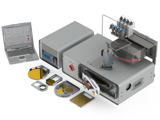
In this study, by the combination of magneto-transport in the van der pauw geometry, tHz time-domain spectroscopy mapping and calibrated Kelvin probe force microscopy a new methodology in measurements of the electrical properties of graphene is developed. Das-Nano Onyx 2D materials quality-inspector system was applied for the THz-TDS measurement to generate maps of sheet resistance of a whole sample area in a contactless non-destructive measurement.


This figure shows the maps of the local sheet resistance obtained using the Onyx THz-TDS system. From the maps it is evident that the sheet resistance features some spatial inhomogeneities, which highlights the need for a weighted average in order to compare the values to the vdP method. Average conductance and resistance values extracted from the THz maps and their standard deviations are summarised in the Table.
Reference: C.Melios, et al. towards standardisation of contact and contactless electrical measurements of cVD graphene at the macro-, micro- and nano-scale. 2019
Explore more
- 2D Material
- 2D materials
- 3D
- 3D printing
- 7th South Australia Space Forum
- adhesion
- adhesive bonding
- Aerospace
- AFM
- ALD
- angle etch
- Apiezon
- ATC
- atomfab
- atomic force microscopy
- battery
- benchtop
- Benchtop PVD Deposition System
- Benchtop Thermal Evaporation
- Biocompatibility
- bonding
- bone differentiation
- Bosch Etcher
- cell adhesion
- Characterisation
- Chemical etch
- Chiller
- CMOS
- CMP
- Coating
- cold atmospheric pressure plasma
- Communicator
- Covid-19
- CRYO Instruments
- Cubesat
- Data Analysis
- Deep Silicon Etch
- Dental
- Deposition
- direct imager
- Direct Write Lithography
- direct writing
- directwrite
- dope
- Dry Etcher
- dry etching
- Edwards Vacuum
- Electrical characterisation
- electron microscopes
- electronic devices
- energy harvesting devices
- Etch Process
- Etch Slanted Features
- etching
- Europlasma
- Evaporation
- FlexAL
- Fluxim
- Gas
- Glovebox
- Graphene
- Grease
- HDPE
- Health Centre
- heat exchangers
- Heidelberg Instruments
- heterostructures
- Holograms
- hydrophilicity
- ICP
- ICPMS
- innovation
- installation
- Ion Beam
- Ion beam etching
- ISO9001
- iVacSens
- Lab On Chip
- lithography
- lithography system
- magnetron
- Maskless Aligner
- Maskless Lithography
- maskless stepper
- masklessaligner
- memories
- MEMS
- MEMs Vacuum Sealer
- microfabrication
- Microfuidics
- Microstructures
- MLA150
- MoS2 Monolayer
- Nano technology
- Nano Vacuum
- nano-oscillators
- nanofabrication
- nanofluidics
- nanofrazor
- nanotechnology
- Nanovac AB
- nanovacuum
- navigation
- Nazia Tabassum
- Nnao Vacuum
- NnaoFrazor
- nomoremasks
- NT-MDT
- Oil
- Oncology
- OpAL
- Optical
- optics
- optoelectronics
- Oxford
- Oxford Instrument
- Oxford Instrument Nano Science
- Oxford Instruments
- Oxford Instruments Nano Science
- Oxford Instruments Plasma Technology
- p-n junction
- pattern
- pattern generator
- patterning
- Perovskite Solar Cells
- Perovskites
- photonics
- photovoltaic
- Physical etch
- Piezobrush
- Plasma
- Plasma Cleaner
- Plasma etch
- Plasma Polish
- Plasma Pro 100 Estrelas
- plasma process
- Plasma technology
- plasma treatment
- Plasmaguard
- PlasmaPro
- plastics
- polarity
- Power Device
- Precision Hot Plates
- Pressure
- Process News
- PTIQ software
- PVD
- PZ3
- quantum
- Quantum Device
- Quantum Devices
- quantum dots
- Quantum technology
- Raman
- Rapid Thermal Annealers
- Recirculating Chillers
- Relocation
- Relyon
- Relyon Plasma
- Replace Mask Aligner
- Rotor Gauge
- RTA
- RTP
- scanning probe microscopy
- semiconductor
- SENS4
- SENS4 A/S
- sensor
- sensors
- shear test
- Si deformation
- SiC
- slanted etching
- slanted features
- SmartPirani
- Software
- solar cells
- Solder Reflow Ovens
- Space Mission
- Space research
- Space Simulation
- Specs
- Spectroscopy
- Spintronic
- Sputtering System
- SRG
- start ups
- superconducting qubits
- superconducting single photon detectors
- surface energy
- surface science
- surface treatment
- The ProteoxTM
- Thermal Vacuum Chamber
- thermochemical scanning probe lithography
- thin film deposition
- tHz time-domain
- Titanium
- TPT Wire Bonder
- Transducer
- TVAC
- UniTemp GmbH
- UNSW
- Vacuum
- Vacuum Pumps
- VSS-300 Vacuum Solder System
- Walk Through Booth
- Wax
- webinar
- wettability
- wire bonding
- X-ray