
Plasma processing for fabrication of porous silicon nanoneedles by Nazia Tabassum from Monash university, Australia
Recent advances in biomedical technology involve the use of microneedles made of diverse materials for effective skin delivery. Microneedles consist of vertical arrays of micron-sized projections designed to penetrate the outermost layer of the skin and interface the epidermis and dermis. Microneedles have been demonstrated to facilitate enhanced transdermal delivery of active agents (e.g. macromolecules, nanoparticles, small polar molecules) otherwise impermeable to the skin. However, currently microneedles present number of disadvantages such as limited drug loading capacity and uncontrolled degradation. Recently, the microneedle scale is sizing down to the nano-scale, which could lead to remarkable advantages. Nanoneedles, i.e. micron-sized needles integrating nanoscale features, are particularly promising because of their increased surface area, reduced invasiveness, and pain-free administration. However, precise control of the over degradation rate of micro/ nanoneedles within the skin remains a great challenge.
Nazia Tabassum from Monash university and her team have developed porous silicon nanoneedles (pSiNNs) with tunable porosity, biodegradability and mechanical strength for non-invasive drug delivery that will improve the treatment of various diseases.
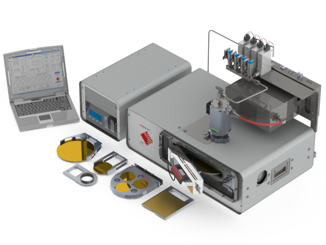
Nanoneedle arrays with a length of 40-50 µm and a tip diameter below 1 µm are fabricated using Oxford Plasma 100 deep reactive ion etching (DRIE) instrument. The Oxford Instruments’ Plasma DRIE allows us to create sharpened nanoneedle projections that are able to puncture the outermost layers of the skin and facilitate the delivery of therapeutic agents. The fabrication process consists of a UV photolithography patterning step followed by dry etching with the DRIE tool. Following, the nanoneedles are posified in a wet etching process by electrochemical anodisation. Further fabrication details are elaborated in the following paragraphs.
Lithography
A chromium mask is used to transfer the defined pattern on a silicon wafer which was coated with positive photoresist. The expressed resist is removed to complete the photolithographic patterning of nanoneedles.
DRIE Process
Si wafers containing photoresist-patterned circles are etched using an Oxford Plasmalab 100 DRIE by performing a Bosch process and by standard dry etching base on RIE. The fabrication of nanoneedle arrays is a three-step process consisting of isotropic sulphur hexafluoride (SF6) step to create a sharp tip, and Bosch process step to obtain cylindrical posts in an anisotropic etching. As a third step, the reshaping of nanoneedles is done with a mixture of SF6 and octafluorocyclobutane (C4F8) gases to obtain sharper tips for enhanced skin penetration.
For full article please click here: - by Nazia Tabassum, Monash University, Australia
Further reference please click here: