Non-destructive electrical characterisation of plasma ALD TiN using THz spectroscopy
Non-destructive electrical characterisation of plasma ALD TiN using THz spectroscopy
Titanium nitride (TiN) is used as a metal gate in complementary metal-oxide-semiconductor (CMOS) technology as it has low resistivity and is compatible
with gate dielectrics.1 TiN has also found new uses in superconducting quantum devices, both as a resonator material2 and for superconducting 3D
interconnects such as through silicon vias3 and as the underbump metallization for chip bonding4 as the field matures and moves towards higher performance materials, including TiN, NbN, and NbTiN. In addition, TiN is still frequently used as a wear resistant coating, and barrier layer for copper diffusion due to its chemical and thermal stability.5 Traditionally TiN was deposited using physical
vapour deposition techniques which suffer from a poor step coverage in deep contacts and via trenches due to shadowing effects, especially in high
aspect ratio structures. Atomic layer deposition (ALD) is a thin film deposition technique which allows for Å-level control of the film thickness, excellent uniformity, and conformal coating of high aspect ratio features. The deposition of thin films of TiN by ALD has been reported using various precursors such as titaniumtetrachloride (TiCl4),6 and tetrakis (dimethylamino) titanium (Ti(N(CH3)2)4, TDMAT).5, 7, 8 Nevertheless, optimization of film growth and
the electrical properties and their uniformities are often required. Ideally, non-destructive characterisation of thickness and electrical uniformity across the entire surface covered by the deposition can be done to ensure the quality
of the final film. This white paper will demonstrate a non-destructive electrical characterisation of plasma atomic layer deposited TiN on 200 mm wafers using THz Spectroscopy.
Equipment and process
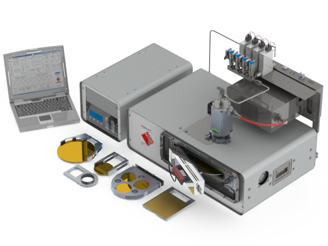
In this work, TiN layers were deposited by plasma enhanced ALD (PEALD) using alternate dosing of TDMAT and a N2/H2 mixed plasma in the Oxford Instruments FlexAL® remote ICP plasma ALD system (figure 1, https://plasma.oxinst.com/ products/ald/flexal-ald). TiN films were deposited
on 200 mm Si(100) wafers at a deposition temperature of 350 ºC with the TDMAT precursor delivered to the reaction chamber at 70 ºC.

Thickness uniformity characterisation
The TiN film thickness, and refractive index uniformity was measured using an ex-situ (visible to near infrared 245–1700 nm) spectroscopic ellipsometer (Woollam M-2000). Good TiN film uniformity of ±3% was measured across the
200 mm Si wafer (Figure 2).

Non-contact electrical resistivity mapping
The 4 point-probe method (4PP) is one of the most well-established and known methods to measure the resistivity of thin-films and other on-wafer materials in the electronics industry. The 4PP is a contact and local measurement method. The contact requirement can cause damage on the surface of the samples. The local measurement provides a value corresponding to the least resistance path across the electrodes within the area defined by the 4 probes. These features
represent a challenge to scale the use of 4PP for mapping the entire surface of large-area wafers, especially in production environments.
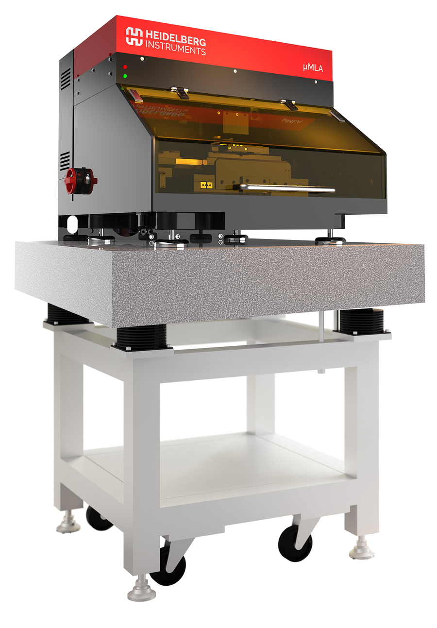
In this work we employ state-of-the-art Terahertz wave technology to overcome all the challenges affecting the 4PP. The Onyx system commercialized by das Nano (figure 3, http://www. das-nano.com/onyx) is a robust and industrialgrade
Terahertz time-domain spectroscopy system co-developed with the leading Terahertz group at the Fraunhofer Institute for Industrial Mathematics (ITWM) to implement a reliable, accurate and easy to use system capable to be operated with minimal operator training and no sample preparation.

Onyx has been tested on a variety of substrates, including quartz, soda-lime glass, silicon, SiC, SiO2, sapphire, cellulose, paper, PET, NbC, AZO, Ge,
Sb, etc. and on a variety of materials, including graphene (mono-layer, bi-layer, flakes, oxide, stacked), ZnO, PEDOT, ITO, CNT, photo-resins,
GaN, Ag inks, etc. The Onyx system is also capable of characterizing new substrates and storing the information in a user-custom database.
Figure 4 shows a 22 nm TiN layer deposited by Oxford Instruments' PEALD and characterized by the Onyx system. This sample presents an average resistivity value of 310 μΩ.cm with a variation of 4% across the entire wafer. The TiN film thickness uniformity (±3%) measured by ellipsometry and resistivity uniformity (4%) characterised using the Onyx system is very well correlated. Noted that 4PP single point measurements yielded higher values of resistivity which can be attributed to the effects of grain boundaries.9 Nevertheless, the Onyx systems
allows for a very fast inspection of the uniformity of the electrical resistivity.

In summary, we demonstrate the deposition of conductive TiN by PEALD across a 200 mm wafer with good thickness and resistivity uniformity by non-contact characterisation techniques (ellipsometry and Onyx THz spectroscopy). The
use of such non-destructive analysis techniques that allow rapid, automated measurements of ALD films is crucial for both process development and high throughput applications.


