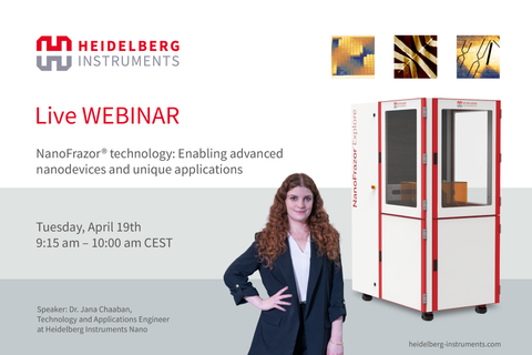
Webinar on NanoFrazor® technology: Enabling advanced nanodevices and unique applications
Join the Live Webinar!
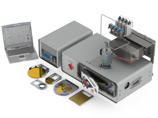
The NanoFrazor uses thermal scanning probe lithography (t-SPL) for the simultaneous patterning and inspection of nanoscale structures, as well as direct laser sublimation (DLS) for mix & match lithography on a surface, namely on thermal resists. The NanoFrazor technology has proven its value as an enabler of novel ultra-high resolution nanodevices, as well as an asset for improving the performance of existing device concepts. In doing so, the NanoFrazor is establishing itself as a mature direct-write nanolithography tool, as well as a complementary extension to other mask-less nanolithography methods such as electron beam lithography (EBL).
The range of applications for t-SPL is very broad, spanning from ultra-high resolution 2D and 3D patterning, to chemical and physical modification of matter at the nanoscale. Nanometer-precise markerless overlay and non-invasiveness to sensitive materials are among the key strengths of the technology. The overlay is shown to work with sub-5nm precision even for nanowires and 2D material flakes that are buried under resist layers, thanks to the highly sensitive in-situ reading capability of the NanoFrazor tool. These unique capabilities allow for the realization of novel nanodevices with emerging 1D and 2D materials, and for nanometer-precise 3D (grayscale) surfaces in optics and fluidics.
In this live webinar, Dr. Jana Chaaban will explain the working principle of the NanoFrazor lithography, and highlight key applications that utilize the unique patterning capabilities of the NanoFrazor technology.
Date: Tuesday, April 19, 2022
Time: 9:15 am CEST
Duration: approx. 45 minutes
Presenter: Dr. Jana Chaaban, Technology and Applications Engineer at Heidelberg Instruments Nano
There will also be a Q&A session at the end of the webinar to address any questions you may have.
Register Here
Explore more
- 2D Material
- 2D materials
- 3D
- 3D printing
- 7th South Australia Space Forum
- adhesion
- adhesive bonding
- Aerospace
- AFM
- ALD
- angle etch
- Apiezon
- ATC
- atomfab
- atomic force microscopy
- battery
- benchtop
- Benchtop PVD Deposition System
- Benchtop Thermal Evaporation
- Biocompatibility
- bonding
- bone differentiation
- Bosch Etcher
- cell adhesion
- Characterisation
- Chemical etch
- Chiller
- CMOS
- CMP
- Coating
- cold atmospheric pressure plasma
- Communicator
- Covid-19
- CRYO Instruments
- Cubesat
- Data Analysis
- Deep Silicon Etch
- Dental
- Deposition
- direct imager
- Direct Write Lithography
- direct writing
- directwrite
- dope
- Dry Etcher
- dry etching
- Edwards Vacuum
- Electrical characterisation
- electron microscopes
- electronic devices
- energy harvesting devices
- Etch Process
- Etch Slanted Features
- etching
- Europlasma
- Evaporation
- FlexAL
- Fluxim
- Gas
- Glovebox
- Graphene
- Grease
- HDPE
- Health Centre
- heat exchangers
- Heidelberg Instruments
- heterostructures
- Holograms
- hydrophilicity
- ICP
- ICPMS
- innovation
- installation
- Ion Beam
- Ion beam etching
- ISO9001
- iVacSens
- Lab On Chip
- lithography
- lithography system
- magnetron
- Maskless Aligner
- Maskless Lithography
- maskless stepper
- masklessaligner
- memories
- MEMS
- MEMs Vacuum Sealer
- microfabrication
- Microfuidics
- Microstructures
- MLA150
- MoS2 Monolayer
- Nano technology
- Nano Vacuum
- nano-oscillators
- nanofabrication
- nanofluidics
- nanofrazor
- nanotechnology
- Nanovac AB
- nanovacuum
- navigation
- Nazia Tabassum
- Nnao Vacuum
- NnaoFrazor
- nomoremasks
- NT-MDT
- Oil
- Oncology
- OpAL
- Optical
- optics
- optoelectronics
- Oxford
- Oxford Instrument
- Oxford Instrument Nano Science
- Oxford Instruments
- Oxford Instruments Nano Science
- Oxford Instruments Plasma Technology
- p-n junction
- pattern
- pattern generator
- patterning
- Perovskite Solar Cells
- Perovskites
- photonics
- photovoltaic
- Physical etch
- Piezobrush
- Plasma
- Plasma Cleaner
- Plasma etch
- Plasma Polish
- Plasma Pro 100 Estrelas
- plasma process
- Plasma technology
- plasma treatment
- Plasmaguard
- PlasmaPro
- plastics
- polarity
- Power Device
- Precision Hot Plates
- Pressure
- Process News
- PTIQ software
- PVD
- PZ3
- quantum
- Quantum Device
- Quantum Devices
- quantum dots
- Quantum technology
- Raman
- Rapid Thermal Annealers
- Recirculating Chillers
- Relocation
- Relyon
- Relyon Plasma
- Replace Mask Aligner
- Rotor Gauge
- RTA
- RTP
- scanning probe microscopy
- semiconductor
- SENS4
- SENS4 A/S
- sensor
- sensors
- shear test
- Si deformation
- SiC
- slanted etching
- slanted features
- SmartPirani
- Software
- solar cells
- Solder Reflow Ovens
- Space Mission
- Space research
- Space Simulation
- Specs
- Spectroscopy
- Spintronic
- Sputtering System
- SRG
- start ups
- superconducting qubits
- superconducting single photon detectors
- surface energy
- surface science
- surface treatment
- The ProteoxTM
- Thermal Vacuum Chamber
- thermochemical scanning probe lithography
- thin film deposition
- tHz time-domain
- Titanium
- TPT Wire Bonder
- Transducer
- TVAC
- UniTemp GmbH
- UNSW
- Vacuum
- Vacuum Pumps
- VSS-300 Vacuum Solder System
- Walk Through Booth
- Wax
- webinar
- wettability
- wire bonding
- X-ray