Heidelberg Instruments webinar recordings are now available
The Heidelberg Instruments webinar recordings are now live!
Please see below the links.
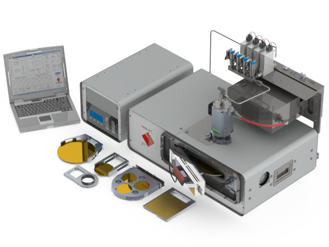
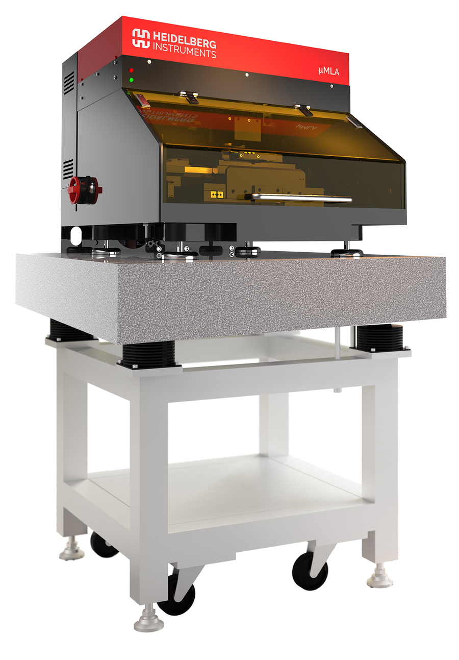
MLA Direct Laser Writer Webinar
Maskless Aligner - Fast prototyping without photo masks
Webinar description: The Maskless Aligner series was first introduced in 2015. Since then, the maskless technology has become firmly established in research labs worldwide as well as in many small to mid-volume micro fabrication facilities. Application areas include MEMS, microfluidics, micro-optics, sensors, electronic components and many more. This webinar will give you an insight into our maskless lithography technology with emphasis on our maskless aligner series.
Webinar recording link here
DWL Greyscale Laser Lithography Webinar
Grayscale Laser Lithography with Heidelberg Instruments DWL Series
Webinar description: Grayscale lithography is used to create three-dimensional micro- and nanostructures with height gradients, enabling the fabrication of textured surfaces with micro- and nano-topographies. In laser lithography, the CAD virtual landscape is mapped to the system’s gray values where each value corresponds to an exposure intensity level. With up to 1000 gray levels and 65000 intensities, 2.5D topographies can be realized, which are required for micro-optical elements such as Fresnel lenses, blazed gratings, micro-lenses but also for other areas such as MEMS, MOEMS or microfluidics.
Webinar recording link here
ULTRA Lithography Webinar
ULTRA Semiconductor photomask Lithography with Heidelberg Instruments
Webinar description: Nano Vacuum Australia & New Zealand is proud to share the Heidelberg Instruments ULTRA Semiconductor photomask Lithography webinar. This webinar will give a technical introduction of the Heidelberg Instruments Ultra Laser Writer. The Ultra technology has evolved from our well established line of Volume Pattern Generators and is used in production of mature semiconductor photomasks as well as for direct write applications.
NanoFrazor – A Nanolithography Tool for 2D & 3D devices Webinar
Webinar description: Nano Vacuum Australia & New Zealand is proud to share the Heidelberg Instruments NanoFrazor lithography systems webinar.NanoFrazor lithography systems were developed as a first true alternative or extension to standard mask-less nanolithography methods like electron beam lithography (EBL). In contrast to EBL they are based on thermal scanning probe lithography (t-SPL). Here a heatable ultra-sharp probe tip with an apex of a few nm is used for patterning and simultaneously inspecting complex nanostructures[1]. The heat impact from the probe on a thermal responsive resist generates those high-resolution nanostructures. The patterning depth of each individual pixel can be controlled with better than 1 nm precision using an integrated in-situ metrology method.
Webinar recording link here