Direct-write lithography for holograms
Development of the Holograms-based Security Technology is defined by the tools at hand
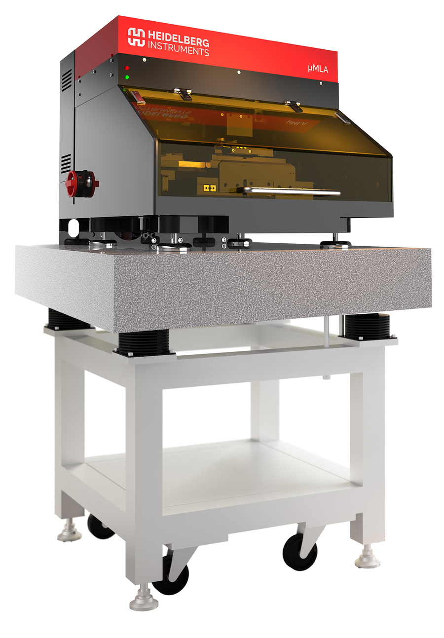
Heidelberg Instruments provides advanced direct-write lithography solutions for more than 35 years, in laser lithography and produces tools from simple table-top R&D systems to industrial-scale wafer writers. Each tool can be equipped with different write-heads to match the resolution and speed requirements of the customer. Direct-write laser lithography uses the laser beam to expose the resist without a mask, patterning a structure line-by-line or in a vector mode, known as maskless lithography.
ADVANTAGE
- Completely eliminates the need for masks
- Rapid prototyping (a few days instead of months)
- Save costs and time (no masks need to be ordered and maintained)
DWL & MLA series :
The capabilities of the direct-write lithography are well-suited for holographic applications of any complexity. Most hologram types require grayscale lithography (DOE's, Fresnell lenses, blazed gratings). DWL series from Heidelberg Instruments are extremely well suited for this task (Fig. 1) and can be used to produce high-quality master molds for replication. The master molds for the so-called binary structures (e.g. lines and spaces as in Fig. 2-3) can be patterned using Heidelberg instruments’ MA150 or written directly on the substrates by MLA300.

Fig. 1. Fresnel Holograms. A: Source .stl fine of a 3D structure and the resulting hologram with apparently deep relief in a very thin layer of resist (~10µm). Example of Fresnel approach. B-C: A half-sphere with a 90 μm radius is cut with a 30μm-pitch grid. D: Within each square of the grid, the plane tangent to the 3D structure is calculated. E: Resulting planes are vertically sliced, similar to a Fresnel lens. Image courtesy: Heidelberg Instruments.

Fig. 2. “Bright” holograms. Similar to the Blazed Grating Hologram, lines and spaces can produce the effect of high color contrast and brightness in a grayscale image. A: Lines and spaces gratings with different orientations in the XY plane diffract the light differently. As a result, different gray values (from the input image) create different colors. Each pixel is replaced by a 10 x 10 μm² square composed of lines and spaces (1 μm pitch). Angle of "lines & spaces" pattern in the XY plane is determined by BMP gray value. B: A bright image, where colors change with the viewing angle. Top left: only the pitch varies with the gray value of the input image. Top right: only the XY angle of a fixed pitch grating varies with the gray value of the input image. Bottom left and right: the pitch and the XY angle of the grating vary with the gray value of the input image. Image courtesy: Heidelberg Instruments.

Fig. 3. Realistic color holograms. Gratings in a thin layer of resist (here 500 nm) can recreate a color image without pigments. A: Schematic of grating structures for different colors. Each pixel is transformed into a 30 x 30 μm² area. Each square is divided into 3 rectangles of 30 x 10 μm2 with varying pitch corresponding to the RGB values. B: Depending on the incoming angle of the illumination (white light) and on the viewing angle of the observer, a certain pitch gives a certain color effect. C-D: The same structure at different viewing angles. Pixels in images shown here have the same pitch/RGB correspondence but the XY angle is different: Top left: XY angle=45°, the colors are not clearly reproduced. Top right: XY angle= 90°, with the illumination angle and viewing angle almost nothing is visible. Bottom left and right: XY angle=0° (horizontal), with the illumination angle and viewing angle, the original colors are reproduced. Images courtesy: Heidelberg Instruments.
NanoFrazor:
It uses an ultra-sharp heatable cantilever to remove thermal resist and to simultaneously read-out the resulting pattern. This approach can reliably produce binary and grayscale patterns down to a few nm in lateral dimensions. (Fig. 4)

Fig. 4. Nanoscale master molds patterned using NanoFrazor technology. A: Computer-generated multilevel hologram in PPA resist. B: An atomic force microscopy image of a 3D hologram pattern in PPA resist. B Image courtesy Heidelberg Instruments Nano, Hologram design: Prof. J. Dong, Sun Yat-Sen University, China.
As compared to electron beam lithography, NanoFrazor technology doesn’t suffer from charging effects and doesn’t require vacuum.
For more information download Direct-write lithography for holograms or contact info@nanovactech.com


