Atomic Layer Deposition for Quantum Devices
As the transistor gave rise to the information age, quantum technology has the potential to be the next great leap forward. Quantum technology is the application of quantum physics for real-world applications, such as quantum computing, sensing, navigation and communication.
Conventional methods for depositing superconductors include sputtering, pulsed laser deposition (PLD), and chemical vapour deposition (CVD). However, these methods can suffer from drawbacks including a lack of thickness control, poor uniformity and high impurity content.
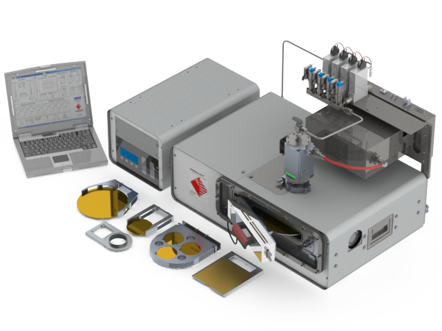
Atomic layer deposition (ALD) is much more beneficial for thin-film deposition due to its ability to produce films with high purity, precise thickness control, conformal coating in high aspect ratio structures, and uniformity over large-area substrates.
The properties of the materials used to produce quantum technology is of paramount importance to its operation. It has been shown that ALD can allow for fine control of these properties such as composition, resistance, Tc and film stress. Thus, ALD can be a driving force behind the development of technologies for quantum applications and the ability of Oxford Instruments' ALD tools to apply a bias during processes could be a route to further enhance the materials used in quantum technology.
For more information on ALD please download brochure, visit products or contact Nano Vacuum Australia & New Zealand at: info@nanovactech.com
Explore more
- 2D Material
- 2D materials
- 3D
- 3D printing
- 7th South Australia Space Forum
- adhesion
- adhesive bonding
- Aerospace
- AFM
- ALD
- angle etch
- Apiezon
- ATC
- atomfab
- atomic force microscopy
- battery
- benchtop
- Benchtop PVD Deposition System
- Benchtop Thermal Evaporation
- Biocompatibility
- bonding
- bone differentiation
- Bosch Etcher
- cell adhesion
- Characterisation
- Chemical etch
- Chiller
- CMOS
- CMP
- Coating
- cold atmospheric pressure plasma
- Communicator
- Covid-19
- CRYO Instruments
- Cubesat
- Data Analysis
- Deep Silicon Etch
- Dental
- Deposition
- direct imager
- Direct Write Lithography
- direct writing
- directwrite
- dope
- Dry Etcher
- dry etching
- Edwards Vacuum
- Electrical characterisation
- electron microscopes
- electronic devices
- energy harvesting devices
- Etch Process
- Etch Slanted Features
- etching
- Europlasma
- Evaporation
- FlexAL
- Fluxim
- Gas
- Glovebox
- Graphene
- Grease
- HDPE
- Health Centre
- heat exchangers
- Heidelberg Instruments
- heterostructures
- Holograms
- hydrophilicity
- ICP
- ICPMS
- innovation
- installation
- Ion Beam
- Ion beam etching
- ISO9001
- iVacSens
- Lab On Chip
- lithography
- lithography system
- magnetron
- Maskless Aligner
- Maskless Lithography
- maskless stepper
- masklessaligner
- memories
- MEMS
- MEMs Vacuum Sealer
- microfabrication
- Microfuidics
- Microstructures
- MLA150
- MoS2 Monolayer
- Nano technology
- Nano Vacuum
- nano-oscillators
- nanofabrication
- nanofluidics
- nanofrazor
- nanotechnology
- Nanovac AB
- nanovacuum
- navigation
- Nazia Tabassum
- Nnao Vacuum
- NnaoFrazor
- nomoremasks
- NT-MDT
- Oil
- Oncology
- OpAL
- Optical
- optics
- optoelectronics
- Oxford
- Oxford Instrument
- Oxford Instrument Nano Science
- Oxford Instruments
- Oxford Instruments Nano Science
- Oxford Instruments Plasma Technology
- p-n junction
- pattern
- pattern generator
- patterning
- Perovskite Solar Cells
- Perovskites
- photonics
- photovoltaic
- Physical etch
- Piezobrush
- Plasma
- Plasma Cleaner
- Plasma etch
- Plasma Polish
- Plasma Pro 100 Estrelas
- plasma process
- Plasma technology
- plasma treatment
- Plasmaguard
- PlasmaPro
- plastics
- polarity
- Power Device
- Precision Hot Plates
- Pressure
- Process News
- PTIQ software
- PVD
- PZ3
- quantum
- Quantum Device
- Quantum Devices
- quantum dots
- Quantum technology
- Raman
- Rapid Thermal Annealers
- Recirculating Chillers
- Relocation
- Relyon
- Relyon Plasma
- Replace Mask Aligner
- Rotor Gauge
- RTA
- RTP
- scanning probe microscopy
- semiconductor
- SENS4
- SENS4 A/S
- sensor
- sensors
- shear test
- Si deformation
- SiC
- slanted etching
- slanted features
- SmartPirani
- Software
- solar cells
- Solder Reflow Ovens
- Space Mission
- Space research
- Space Simulation
- Specs
- Spectroscopy
- Spintronic
- Sputtering System
- SRG
- start ups
- superconducting qubits
- superconducting single photon detectors
- surface energy
- surface science
- surface treatment
- The ProteoxTM
- Thermal Vacuum Chamber
- thermochemical scanning probe lithography
- thin film deposition
- tHz time-domain
- Titanium
- TPT Wire Bonder
- Transducer
- TVAC
- UniTemp GmbH
- UNSW
- Vacuum
- Vacuum Pumps
- VSS-300 Vacuum Solder System
- Walk Through Booth
- Wax
- webinar
- wettability
- wire bonding
- X-ray