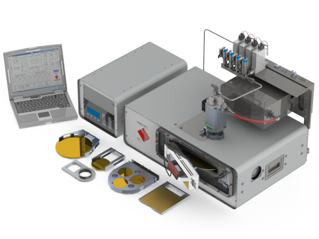

Application of NanoFrazor in fabrication of p-n junctions in 2D materials
In the recent Nature Communications publication, Prof. Elisa Riedo and her team demonstrated the integration of NanoFrazor’s heated tip with a HCl/H2O or N2 reactive gas cell to reach nanoscale management of defects in 2D material like monolayer MoS2. As a result, they were able to create p-n junctions with the rectifying ratio of over 10^4 in one-step fabrication.
Defect nanoengineering combined with thermochemical scanning probe lithography capability of imaging, cutting and locally doping the flakes can be applied for various applications such as optoelectronics, flexible electronics and energy harvesting devices where devices with regions of various polarity are needed.

a Schematics of the tc-SPL experiment. b KPFM image of a three-layer exfoliated MoS2 flake, where a pattern of 1.2 × 0.3 µm2 has been produced at a high temperature (T = 873 K) and at a scan rate of ν = 0.024 µm s−1 in a HCl/H2O-rich environment (scale bar: 1 µm, z scale: 160 mV). This pattern is highlighted by white boxes in the image. Top inset shows the cross-section profile of the KPFM image across the pattern as indicated with a solid line in (b), specifically we plot both the contact potential difference (ΔCPD = CPDpattern–CPDnon-patterned) and the thickness fluctuation. Bottom inset shows the AFM topography of the same pristine flake (scale bar: 1 µm, z scale: 25 nm). c Work-function difference between the tc-SPL pattern and the nonpatterned MoS2 flake ΔΦKPFM = (ΔΦpattern –ΔΦnon-pattern) vs. inverse patterning scan rate, and the corresponding data fit with Eq. (1) (shown as a gray line in (c). The error bar is the standard deviation of KPFM data within the area of analysis. d Raman spectra collected inside (data in light blue) and outside (data in black) a tc-SPL heated pattern in single-layer exfoliated MoS2.
Reference: Zheng et al., Spatial defects nanoengineering for bipolar conductivity in MoS2, Nat. Commun, 2020.