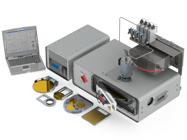
Application of Maskless Aligner MLA150 for patterning conductive tracks
The result of Heidelberg MLA150 Maskless Aligner is presented in a novel study on Photolithography–Enabled Direct Patterning of Liquid Metals by Prof Kalantar-Zadeh and his team.
Non-contact exposure, outstanding ease of use, and high speed make the Maskless Aligner MLA150 the ideal tool in rapid prototyping environments, for low- to mid-volume production, and in Research & Development.
Maskless photolithography eliminates the need for a photomask: The system exposes the pattern directly onto the resist-covered surface. Should design modifications be required, these can be quickly implemented by changing the CAD layout, resulting in much-reduced cycle-times. You will also benefit from a fast, automated front- and backside alignment procedure as well as the outstanding speed. The application areas of the MLA150 include life sciences, MEMS, micro-optics, semiconductors, sensors, actuators, MOEMS, material research, nano-tubes, and graphene.
Download brochure here.

Explore more
- 2D Material
- 2D materials
- 3D
- 3D printing
- 7th South Australia Space Forum
- adhesion
- adhesive bonding
- Aerospace
- AFM
- ALD
- angle etch
- Apiezon
- ATC
- atomfab
- atomic force microscopy
- battery
- benchtop
- Benchtop PVD Deposition System
- Benchtop Thermal Evaporation
- Biocompatibility
- bonding
- bone differentiation
- Bosch Etcher
- cell adhesion
- Characterisation
- Chemical etch
- Chiller
- CMOS
- CMP
- Coating
- cold atmospheric pressure plasma
- Communicator
- Covid-19
- CRYO Instruments
- Cubesat
- Data Analysis
- Deep Silicon Etch
- Dental
- Deposition
- direct imager
- Direct Write Lithography
- direct writing
- directwrite
- dope
- Dry Etcher
- dry etching
- Edwards Vacuum
- Electrical characterisation
- electron microscopes
- electronic devices
- energy harvesting devices
- Etch Process
- Etch Slanted Features
- etching
- Europlasma
- Evaporation
- FlexAL
- Fluxim
- Gas
- Glovebox
- Graphene
- Grease
- HDPE
- Health Centre
- heat exchangers
- Heidelberg Instruments
- heterostructures
- Holograms
- hydrophilicity
- ICP
- ICPMS
- innovation
- installation
- Ion Beam
- Ion beam etching
- ISO9001
- iVacSens
- Lab On Chip
- lithography
- lithography system
- magnetron
- Maskless Aligner
- Maskless Lithography
- maskless stepper
- masklessaligner
- memories
- MEMS
- MEMs Vacuum Sealer
- microfabrication
- Microfuidics
- Microstructures
- MLA150
- MoS2 Monolayer
- Nano technology
- Nano Vacuum
- nano-oscillators
- nanofabrication
- nanofluidics
- nanofrazor
- nanotechnology
- Nanovac AB
- nanovacuum
- navigation
- Nazia Tabassum
- Nnao Vacuum
- NnaoFrazor
- nomoremasks
- NT-MDT
- Oil
- Oncology
- OpAL
- Optical
- optics
- optoelectronics
- Oxford
- Oxford Instrument
- Oxford Instrument Nano Science
- Oxford Instruments
- Oxford Instruments Nano Science
- Oxford Instruments Plasma Technology
- p-n junction
- pattern
- pattern generator
- patterning
- Perovskite Solar Cells
- Perovskites
- photonics
- photovoltaic
- Physical etch
- Piezobrush
- Plasma
- Plasma Cleaner
- Plasma etch
- Plasma Polish
- Plasma Pro 100 Estrelas
- plasma process
- Plasma technology
- plasma treatment
- Plasmaguard
- PlasmaPro
- plastics
- polarity
- Power Device
- Precision Hot Plates
- Pressure
- Process News
- PTIQ software
- PVD
- PZ3
- quantum
- Quantum Device
- Quantum Devices
- quantum dots
- Quantum technology
- Raman
- Rapid Thermal Annealers
- Recirculating Chillers
- Relocation
- Relyon
- Relyon Plasma
- Replace Mask Aligner
- Rotor Gauge
- RTA
- RTP
- scanning probe microscopy
- semiconductor
- SENS4
- SENS4 A/S
- sensor
- sensors
- shear test
- Si deformation
- SiC
- slanted etching
- slanted features
- SmartPirani
- Software
- solar cells
- Solder Reflow Ovens
- Space Mission
- Space research
- Space Simulation
- Specs
- Spectroscopy
- Spintronic
- Sputtering System
- SRG
- start ups
- superconducting qubits
- superconducting single photon detectors
- surface energy
- surface science
- surface treatment
- The ProteoxTM
- Thermal Vacuum Chamber
- thermochemical scanning probe lithography
- thin film deposition
- tHz time-domain
- Titanium
- TPT Wire Bonder
- Transducer
- TVAC
- UniTemp GmbH
- UNSW
- Vacuum
- Vacuum Pumps
- VSS-300 Vacuum Solder System
- Walk Through Booth
- Wax
- webinar
- wettability
- wire bonding
- X-ray