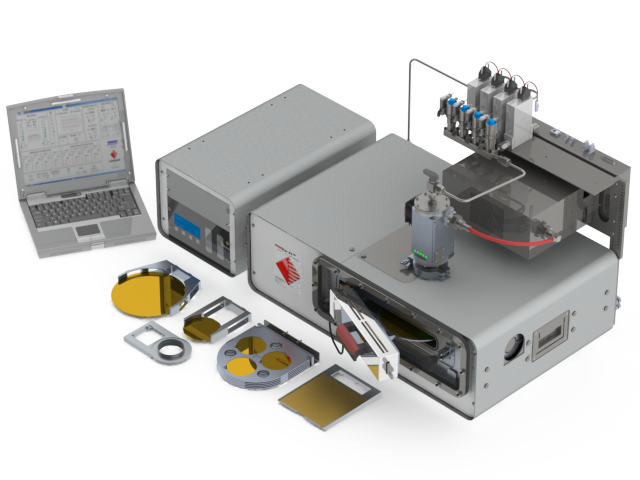

The PlasmaPro 100 Atomic Layer Etching system delivers precise process control of etching for next-generation semiconductor devices. Specially designed for processes such as recess etching for GaN HEMT applications and nanoscale layer etching, the system's digital/cyclical etch process offers low damage, smooth surfaces.
-
Digital/Cyclical etch process – etching equivalent of ALD
-
Low damage
-
Smooth etch surface
-
Superb etch depth control
-
Ideal for nanoscale layer etching (e.g. 2D Materials)
-
Wide range of processes and applications
Features & Benefits
As layers become thinner to enable the next-generation semiconductor devices, there is a need for ever more precise process control to create and manipulate these layers. The PlasmaPro 100 ALE delivers this by enhancing our Cobra ICP platform with specialised hardware for atomic layer etching.
-
Delivers reactive species to the substrate, with a uniform high conductance path through the chamber - Allows a high gas flow to be used while maintaining low pressure
-
Variable height electrode - Utilises the 3-dimensional characteristics of the plasma and accommodate substrates up to 10mm thick at optimum height
-
Wide temperature range electrode (-150°C to +400°C) which can be cooled by liquid nitrogen, a fluid re-circulating chiller or resistively heated - An optional blow out and fluid exchange unit can automate the process of switching modes
-
A fluid controlled electrode fed by a re-circulating chiller unit - Excellent substrate temperature control
-
RF powered showerhead with optimised gas delivery - Provides uniform plasma processing with LF/RF switching allowing precise control of film stress
-
ICP source sizes of 65 mm, 180 mm, 300 mm - Delivers process uniformity up to 200 mm wafers
-
High pumping capacity - Gives wide process pressure window
-
Wafer clamping with He backside cooling - Optimum wafer temperature control
Applications
- Low damage GaN HEMT recess etch for power electronics and RF devices
- 2D materials patterning/thinning
- Nanostructured SiO2, Si, SiN
- III-V materials
- Solid-state lasers InP etch
- VCSEL GaAs/AlGaAs etch
- Silicon Bosch and cryo-etch processes
- Hard mask deposition and etch for high brightness LED production
- SiO2 and quartz etch
Upgrades/Accessories
Gas pod - incorporate extra gas lines and allow greater flexibility
Logviewer software - datalogging software allows realtime graphing and post run analysis
Optical end point detectors - an important tool for achieving optimal process results
Soft pump - allows the slow pumping down of a vacuum chamber
Turbomolecular vacuum pump - offers superior pumping speeds and higher throughput
X20 Control System - delivers a future proof, flexible and reliable tool with increased system ‘intellect’
Advanced Energy Paramount generator - Offering increased reliability and greater plasma stability
Automatic pressure control - This controller ensures very fast and accurate pressure control
Dual CM gauge switching - provides the ability to utilise two differing ranges of capacitance manometer via a single pressure control valve
LN2 autochangeover unit - enables table cooling fluid to be automatically switched between Liquid Nitrogen (LN2) and Chiller Fluid
Wide temperature range electrode - significant design improvements to increase process performance
You may also like

More from Oxford Instruments Plasma
More from Atomic Layer Etching (ALE) Systems
Recently viewed