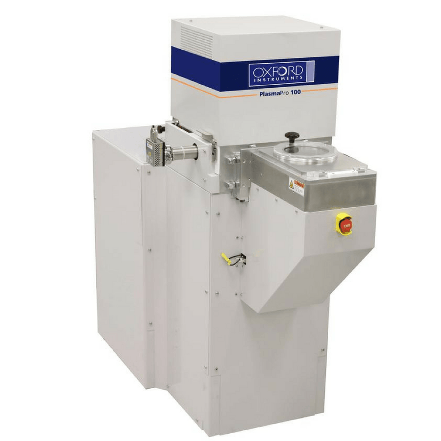
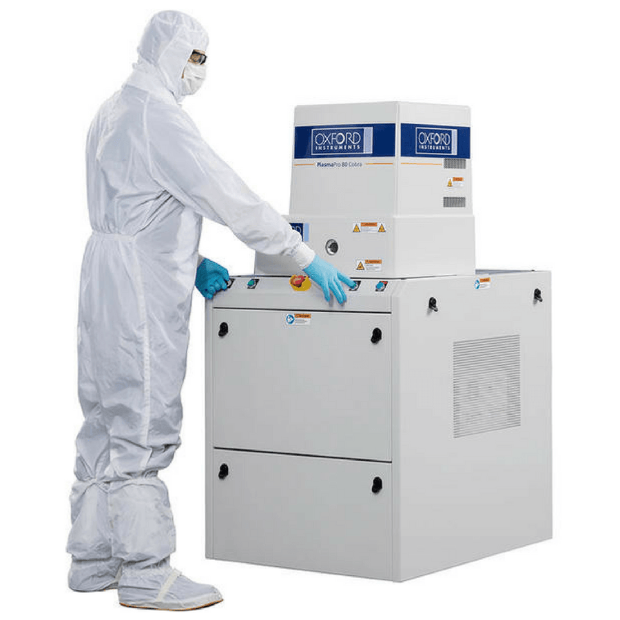
Inductively Coupled Plasma Chemical Vapour Deposition (ICPCVD)
Creation of high density plasmas in the ICP source means this technique delivers deposition of high quality dielectric films at low temperature with low damage. Low temperature deposition means that temperature sensitive films and devices can be processed successfully.

Highlights
- Independent control of ion energy and ion current density
- Typical process pressure: 1- 10 mtorr
- Plasma density: circa 5 x E11 / cm2
- Plasma in contact with the substrate
- Low energy ion current during deposition
- Ion Current (Plasma Density) dependent on ICP power
- ESS (electrostatic screen) for a purely inductive plasma
- ICP is fully automatic (2 RF automatch units)
Features & Benefits
- Excellent quality low damage films at reduced temperatures.
- Typical materials deposited include SiO2, Si3N4 and SiON, Si and SiC at substrate temperatures as low as 5ºC
- ICP source sizes of 65mm, 180mm, 300mm delivering process uniformity up to 200mm wafers
- Electrodes available for temperature ranges from 5ºC to 400ºC
- Patented ICPCVD gas distribution technology
- In situ chamber cleaning with endpointing
ICPCVD Chamber Clean
Our ICPCVD cleaning regime was developed to give reproducible deposition and low particles between mechanical cleans
- Reduced cleaning time
- Higher utilisation through optional interleaved clean
- Accurate endpoint resulting in reduced over-etch of chamber components and increasing their lifetime

High Rate Clean Process Features
- System Utilisation >70%
- SF6 /N2O gas mixture
- Improved End Point control
- Plasma clean results in increased optical intensity with greater endpoint signal/resolution
- Actual plasma clean time depends on film material, film quality and film thickness
Interleaved Clean Mode
- High utilisation
- Highly repeatable deposition rate
- Low added particle counts maintained with clean after every wafer
- > 50 microns between mechanical cleans


