


Workshops Conducted 'NanoFrazor Explore Lithography System For Advanced Fabrication 2D and 3D Nanodevices'
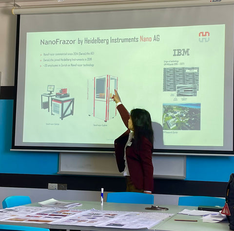
Nano Vacuum was excited to present Heidelberg Instruments workshops on 'NanoFrazor Explore The Revolutionary Lithography System for advanced 2D and 3D Nanodevices' by Dr. ZhengMing Wu, Senior Sales Manager at Heidelberg Instruments.
The workshop highlighted how the application range for the NanoFrazor Explore nanolithography technique is broad spanning from ultra-high resolution 2D and 3D patterning to chemical and physical modification of matter at the nanoscale.
Nano Vacuum would like to mention and thank the diverse set of facilities around Australia and New Zealand that we were hosted at:
The Australian National Fabrication Facility (ANFF) nodes including Melbourne Centre for Nanofabrication, ANFF-Qld, ANFF-WA, ANFF-SA, UNSW and The University of Sydney Nano Institute Sydney Nanoscience Hub. RMIT University, CSIRO NSW, Victorian University of Wellington and Canterbury University
Related publications:
- Optical Fourier Surfaces - Lassaline et al., Nature, 2020
- Thermal scanning probe lithography—a review - Howell et al., Microsystems & Nanoengineering, 2020
- Nanoscale spin-wave circuits based on engineered reconfigurable spin-textures - Albisetti et al., Comm. Phys., 2018

Optical Fourier Surfaces - Lassaline et al., Nature, 2020

Nanoscale spin-wave circuits based on engineered reconfigurable spin-textures - Albisetti et al., Comm. Phys., 2018
